Micro-Electro-Mechanical Systems and its Fabrication
Introduction
Micro-electro-mechanical systems (MEMS) have numerous applications in the field of aeronautical, space, biomedical and automobile industries. MEMS device basically consists of sensors for detection of physical parameters, signal processing/conditioning circuits for converting them to current/voltage levels and an actuator for carrying out required operation/correction. These devices are fabricated on silicon substrate using micro-machining technology. The basic building blocks of sensors and actuators are microstructures such as cantilever beams, diaphragms, bridges, suspended membranes, etc. and fabricated using 'bulk micro machining' or 'surface micro machining' technology. These microstructures being delicate, requires very careful packaging and handling to avoid possible damages. In order to over come this problem, a new technique to form MEMS microstructure several microns below the surface of the silicon wafers. Has been developed. This technique is termed as 'recessed microstructure'
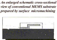
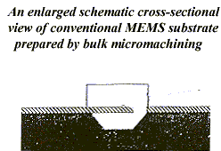
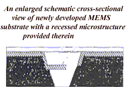
MEMS device is formed in the cavity of the substrate (as a Recessed Microstructure) through a series of machining steps. The semiconductor substrate generally comprises of microcrystalline silicone with a surface oxide layer. The surface may be doped or undoped, depending on the type of MEMS to be formed within the cavity as well as the electronic circuitry to be formed. One or more open cavities are formed after subjecting the substrate to lithography and etching. The substrate is then subjected to reoxidisation followed by further lithography and oxide etching to obtain the first functional level of MEMS. This is is subjected to P power(4) diffusion and subsequently formed by depositing a first layer of a micromachinable material which is also a conductive material. This layer is micromachined and etched to form one or more functional elements of the MEMS. These elements are suitably joined to form functional components like sensors or actuators. MEMS can also be integrated with electronic circuitry (e.g. CMOS, BiCMOS or bipolar electronic circuitry ) Figure 1 shows an enlarged schematic cross-sectional view of conventional MEMS substrate prepared by bulk micromachining Figure 2 shows an enlarged schematic cross-sectional view of conventional MEMS substrate prepared by surface micromachining Figure 3 shows an enlarged schematic cross-sectional view of newly developedl MEMS substrate with a recessed microstructure provided therein.


Salient features
The newly developed process enables easy packaging and handling of MEMS. Further, a number of difficulties faced during conventional surface/bulk machining process, such as, selective etching of sacrificial layer without reacting with other materials, increased use of materials for sacrificial layer, additional etching step required to remove sacrificial layer, increased duration of machining are eliminated.
Prospective Users
Electronic control circuits used for various applications in Aeronautical industry, Chemical industry, Food processing industry, Metallurgical Industry, Automobile, Space, Railways, Defence etc. Micro-sensor applications Radio Frequency (RF) switches
Type of Technology
Electronic Device
Status of IPR Protection
Indian Patent Application No. 39/DEL/2003 dated 13.1.2003 with title "Recessed Microstructure Device and Method of Fabrication Thereof"
Status of Development
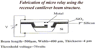
The technology has been demonstrated through the fabrication of micro relay using the recessed cantilever beam structure.(Figure 4)
Keywords
Microstructure, Etching, Micro machining, Sensors
Services offered by Technology Transfer
Know how manual including quality control procedures Process demonstration as developed Consultancy
Developed by
Dr. Prem Pal
Department
Center for Applied Research in Electronics
For further information please contact
Managing Director
Foundation for Innovation and Technology Transfer (FITT)
Indian Institute of Technology, Delhi
Hauz Khas, New Delhi-110016, INDIA
Tel : 91-011-26597167, 26857762, 26581013, 26597153
Fax : 91-011-26851169
E-mail : drkdpn@gmail.com


